Samsung Mass-Produces Silicon Capacitors to Revolutionize AI Semiconductor Market
June 14, 2026
The company frames silicon capacitors as complementary to MLCCs, expanding the embedded substrate market and accelerating adoption in AI servers and data centers.
Its Integrated Stack Capacitor process achieves high capacitance in a small area by deeply etching silicon wafers, boosting performance for AI workloads.
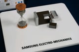
The company has begun full-scale mass production of silicon capacitors, completing a three-product AI semiconductor supply chain with MLCCs and FC-BGA package substrates.
Samsung Electro-Mechanics is mass-producing silicon capacitors to tackle AI semiconductor power and noise challenges, aiming to complete a full advanced components lineup alongside MLCCs and FC-BGA substrates.
A key advantage is dramatically lower parasitic inductance (ESL) by more than 100 times compared with MLCCs, enabling ultra-fast energy delivery and improved signal integrity for AI workloads.
Samsung positions itself as an integrated solutions provider able to supply MLCCs, substrates, and silicon capacitors together, a competitive edge over peers like Murata and TSMC who don’t offer all three.
Silicon capacitors deliver power with high-frequency efficiency, reducing signal interference and enabling stable power delivery in AI GPUs and HBMs.
Market outlook points to a global silicon capacitor market CAGR of about 18% from 2026 to 2031, driven by demand for high-frequency, high-density components in AI infrastructure.
Samsung recently secured a 1.5 trillion won contract to supply silicon capacitors to a global firm, signaling rapid ramp-up and global expansion starting next year.
These devices maintain stable performance across wide temperature ranges, including above 250 degrees Celsius, supporting reliability in harsh environments and aerospace applications.
The silicon capacitor uses a DRAM-inspired hollowed wafer process to maximize surface area, achieving a core storage layer as thin as 10 micrometers for high integration and performance.
Samsung is pursuing a collaborative sales approach that combines MLCC, silicon capacitor, and package solution teams to shorten development cycles and offer on-site voltage and capacity consulting.
Summary based on 2 sources