Revolutionary Metasurface Design Boosts Nonlinear Optical Effects in 2D Crystals for Quantum Photonics
November 23, 2025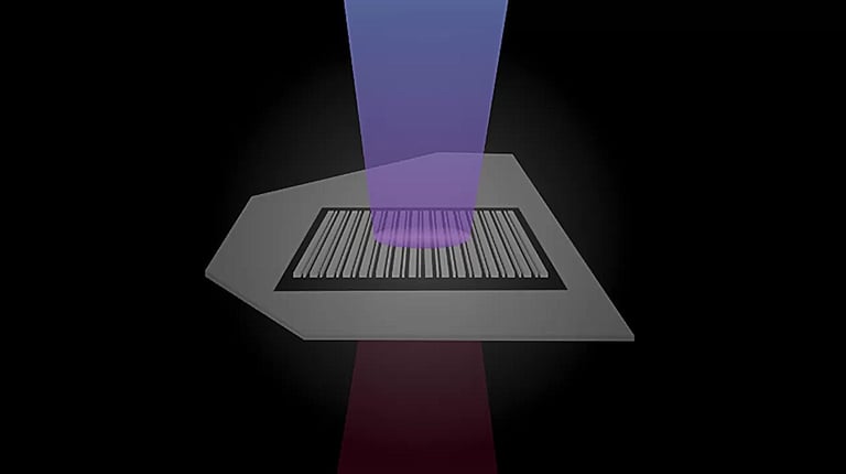
The team demonstrates about a 150-fold increase in second-harmonic generation compared to unpatterned samples, significantly enhancing on-chip quantum light sources.
The metasurface design achieves sub-wavelength thickness (around 160 nanometers) and remains compatible with existing telecommunications networks, pushing toward fully on-chip quantum photonics.
The fabrication is simpler and cheaper than prior methods, using standard cleanroom etching to pattern the metasurface lines on MoS2 flakes.
Theoretical collaborators identified an optimal pattern—periodic lines with alternating widths—to maximize nonlinear response and enable entangled photon pair generation for on-chip quantum photonics.
This pattern optimization supports practical generation of entangled photons and aligns with the goal of scalable quantum technologies.
The work builds on a January 2025 Nature Photonics study that used periodic poling in multilayer MoS2 to generate entangled photon pairs, aiming to power scalable quantum processors with compact qubit sources.
The broader objective is to integrate these high-efficiency, nanoscale nonlinear sources into compact, scalable quantum photonic systems for telecom-compatible, on-chip applications.
Future work will focus on translating enhanced second-harmonic generation into entangled-photon generation and broader on-chip quantum photonic applications.
The core innovation is embedding nanoscale metasurfaces into ultrathin MoS2 to boost nonlinear optical responses and enable efficient on-chip photonics.
Columbia Engineering researchers have embedded metasurfaces into ultrathin transition metal dichalcogenide crystals, notably MoS2, to dramatically boost nonlinear optical effects, achieving high efficiency on 160-nanometer-thick platforms as reported in Nature Photonics.
The metasurface approach uses etched, repeating geometries to induce nonlocal optical properties, enabling strong nonlinear responses in 2D crystals previously limited by their thickness.
Overall impact centers on reducing device size while boosting nonlinear efficiency, paving the way for scalable quantum technologies and moving toward splitting a photon into two entangled photons.
Summary based on 2 sources
Get a daily email with more Science stories
Sources
Phys.org • Nov 22, 2025
Metasurfaces etched into 2D crystals boost nonlinear optical effects at nanoscale
Quantum Zeitgeist • Nov 23, 2025
Engineers Shrink Nonlinear Crystals For Quantum Tech