Breakthrough in 3D Imaging Links Atomic Structures to Advanced Material Engineering
April 30, 2026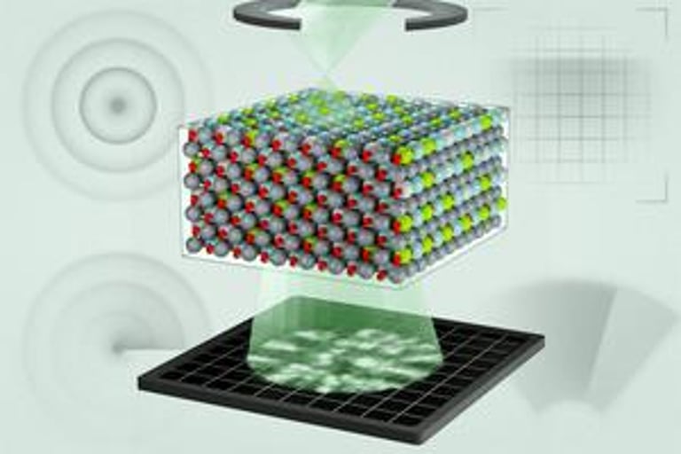
The work demonstrates how electron ptychography can map 3D polar structures in complex, disordered materials and directly connect them with molecular dynamics calculations.
Findings reveal a hierarchical arrangement of chemical and polar structures from atomic to mesoscopic scales, with many polarized regions smaller than prior simulations predicted.
The study shows polarization is modulated by individual chemical species based on atomic charge states, with regions smaller and more correlated than expected.
Overall, polarization structures are hierarchical and more tightly correlated than simulations had anticipated.
Researchers see this approach as a path to engineer advanced materials for improved memory storage, sensing, and energy technologies.
By linking experimental 3D polar structures with dynamic simulations, the study improves predictive modeling of material behavior at the atomic level.
Lead author emphasizes that direct atomic observation enables validation and refinement of computational models with higher fidelity.
Support came from multiple U.S. agencies and MIT.nano facilities, illustrating strong institutional backing for this cutting-edge imaging capability.
Researchers stress that empirical validation is crucial for reliable computational predictions, framing MEP as a feedback loop between theory and experiment.
Collaborative effort involved MIT, several universities worldwide, and funding from the Army Research Laboratory, Office of Naval Research, Department of War, and a National Science Graduate Fellowship.
The material studied is lead magnesium niobate-lead titanate (PMN-PT), whose nanoregions and polarization configurations form a hierarchical mosaic observable with MEP across scales.
The project highlights extensive institutional support for advancing 3D atomic-scale imaging and its applications.
Summary based on 4 sources
Get a daily email with more Science stories
Sources

MIT News | Massachusetts Institute of Technology • Apr 30, 2026
The hidden structure behind a widely used class of materials
EurekAlert! • Apr 30, 2026
The hidden structure behind a widely used class of materials
BIOENGINEER.ORG • Apr 30, 2026
Unveiling the Hidden Framework of a Popular Class of Materials
Mirage News • Apr 30, 2026
Hidden Structure Behind Widely Used Class Of Materials