Samsung's New Hub to Accelerate Advanced Semiconductor Packaging in AI Era
November 1, 2026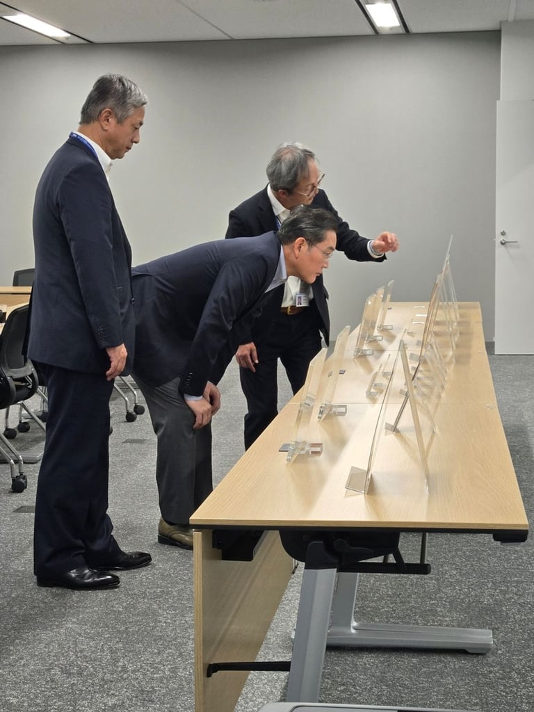

Samsung plans to turn APL into a research collaboration hub that links Samsung’s semiconductor know-how with Japanese materials and equipment suppliers to accelerate development in advanced packaging technologies.
Samsung Electronics Chairman Jay Y. Lee visited the Advanced Package Lab in Yokohama, marking his first public engagement since becoming chairman four years ago on Oct. 27.
Lee stressed that securing advanced packaging technologies is essential to maintaining semiconductor competitiveness in the AI era.
Market context shows momentum in HBM4 and tight CoWoS capacity, creating an opportunity for Samsung to offer integrated memory, logic, and packaging services that could affect suppliers, memory prices, and AI buyers.
There are risks and open questions about headcount and production timelines for glass substrates, plus potential tech and execution risks in scaling wafer bonding and glass substrates, with a necessary handoff from R&D to mass production.
Samsung disclosed in its Q3 earnings that its HBM market share is about 40%, similar to its DRAM share, and announced the HBM4E mass-production timeline for the first half of next year, signaling leadership in this generation.
Lee’s visit follows a pattern of field-oriented leadership, with inspections of core sites to emphasize practical development over ceremonial events.
A key driver is the CoWoS bottleneck at TSMC, prompting Samsung to pursue a second source for packaging and to offer memory, logic, and packaging under one roof.
Developers and AI teams should watch packaging availability, memory per accelerator, and power implications, as advances in packaging can affect accelerator lead times, model sizes, and data-center costs.
Industry analysts caution that while APL’s research could boost competitiveness, translating it into mass-production gains will take time and depend on how quickly results feed into Samsung’s HBM and foundry businesses.
The Cheonan Plant remains central to HBM back-end processes and advanced packaging, with ongoing inspections of production lines and cleanrooms to ensure manufacturing readiness.
FAQs clarify what Lee did, the investment scale, lab opening timeline, technologies researched, why advanced packaging matters for AI, and that the visit does not signal Samsung beat TSMC in packaging or announce new products.
Summary based on 15 sources
Get a daily email with more Tech stories
Sources

The Elec Inc. • Nov 2, 2026
Samsung Chairman Lee Jae-yong Visits Advanced Packaging Research Center in Japan
The Global Giving News • Nov 1, 2026
Lee Jae-yong Links Japanese Materials and Equipment Expertise to AI Chip Technology, Makes First Visit to P...
Shattered • Nov 1, 2026
Samsung Lee in Japan: 3 Packaging Takeaways [2026]
The Korea Herald • Nov 1, 2026
Samsung chief Lee visits Japan chip packaging lab - The Korea Herald