Breakthrough Electron Microscopy Reveals Atomic-Scale Heat Dynamics in Semiconductors
August 26, 2026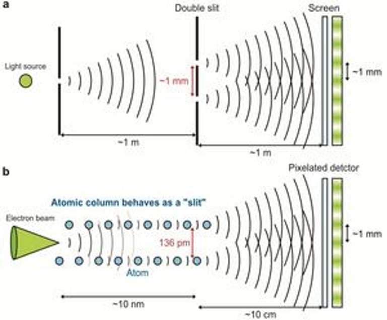

An international team from the University of Tokyo demonstrated an atomic-scale double-slit interference using a focused electron probe to read out vibrations of neighboring silicon atoms, effectively visualizing phonon-related lattice dynamics at the scale of a single atomic bond.
This technique points toward ultra-atomic-resolution electron microscopy that could surpass traditional methods and inform heat-dissipation design and energy efficiency in semiconductor materials.
By examining how the fringe patterns change, researchers can infer the direction and synchronization of atomic vibrations, highlighting regions where heat accumulates or flows less readily.
The work, part of the SHIBATA Ultra-atomic Resolution Electron Microscopy project and conducted with Toma Susi of the University of Vienna, was published in Nature on August 19, 2026.
The study offers a new method for measuring phonons and bonding strength at the atomic level, potentially guiding the engineering of heat conduction in materials and semiconductors.
In the experiment, two adjacent silicon atomic columns spaced 136 picometers apart were treated as a natural double slit, with the resulting interference fringe revealing coordinated vibrations between the neighboring atoms.
Summary based on 1 source
Get a daily email with more Science stories
Source
EurekAlert! • Aug 26, 2026
Observing the vibrations of neighboring atoms with an atomic-scale double slit