Huawei's Bold 5-Year Plan: Semiconductor Leap Amid Sanctions with Tau Scaling Law
May 25, 2026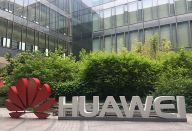


Some observers view the shift toward system efficiency and non-traditional scaling as a viable route to narrowing the gap, yet emphasize the hurdles of cost, power, heat, and integration for broad AI deployments.
Huawei unveils a bold five-year plan to build industry-leading semiconductors under sanctions, using a Tau Scaling Law to push transistor density toward 1.4-nanometer-class performance by 2031, signaling China’s strategic push against restricted access to advanced lithography tools.
A related LogicFolding architecture is slated for upcoming Kirin chips, aiming to shorten wiring inside chips and deliver meaningful performance gains, though independent performance data was not disclosed in the briefing.
Industry observers caution that large-scale viability will require extensive collaboration with data-center operators and equipment makers to translate theory into real-world deployment.
Experts acknowledge Tau Scaling as a credible path but warn about tool access, heat management, and achieving parity with leading nodes; analysts say China may narrow the gap but likely won’t fully match the most advanced nodes soon.
Analysts also highlight ongoing challenges in cost, power, heat, and system integration for cloud AI servers, underscoring that Moore’s Law is being replaced by system-level efficiency efforts.
Huawei invites global collaboration from scientists and industry partners, while noting that practical engagement will be strongest within China due to geopolitical and regulatory factors.
Officials stress that transistor density alone won’t determine leadership; commercial success hinges on yields, power efficiency, packaging, software, and manufacturing economics.
REPS 2.3 aims to cut emissions in transport and electricity by promoting cleaner energy, sustainable mobility, and modernized power infrastructure to support long-term climate targets.
Pronto faces backlash over alleged use of customer recordings to train its AI, reigniting privacy and consent concerns in AI development policies.
Moore’s Law fatigue is cited as motivation, with Tau Scaling positioned as a sustainable path to meet rising computing demands.
Observers will scrutinize Huawei’s feasibility and timeline amid ongoing geopolitical and supply-chain constraints.
Summary based on 47 sources
Get a daily email with more World News stories
Sources

Economic Times • May 25, 2026
Huawei proposes new path for chip development amid US sanctions
The Next Web • May 25, 2026
Huawei unveils ‘Tau Scaling Law’ as China’s workaround for US chip sanctions
Nikkei Asia • May 25, 2026
Huawei says new Kirin chip for phones overcomes US clampdown
Economic Times • May 25, 2026
Huawei proposes new path for chip development amid US sanctions